As Martin confirmed the MPPT-2420-LC hw and fw are capable to work in buck or boost modes.
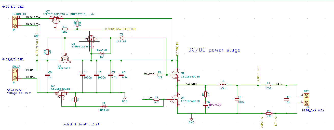
I found interesting to modify the hw and fw in such a way that the device should be capable to charge a battery in buck mode during day time, than in dark condition it should operate in boost mode to supply a high power LED light so energy stored in the battery will be used for lighting.
I opened this topic to share this project with anyone who might be interested in this feature.
I’m sharing my first draft schematics and some thoughts.
The Q2, R2 and D1 are unnecessary and should not be placed for this modification, I’m just planning to leave it there in case the boost feature is not needed or if someone wish to keep the current protection circuit.
For boost mode Q2 S-D should be connected to allow current flow.
To detect day/night conditions I need a way to measure the PV voltage continuously. I thought not to interrupt the SOLAR-, so I’m planning to use the reverse protection from MPPT_Charger_12A.
PV_Voltage output can be used for monitoring purpose.
I added LOAD(LED) output which can be turned on with DCDC_LOAD(LED)_OUT.
I’m planning to use relatively high voltages
for LED’s around 40-50V and current will be around 2-3A so using a P-channel MOSFET shouldn’t be a problem (it’s relatively hight RDS(on) is still OK for this application)
I’ve got some concerns. Not sure if the circuit will work as intended.
Q2 can be used also for boost mode, as it is continuously on as soon as the power stage is switching. It is kept on during off-time of the LS FET by the MOSFET’s internal gate capacity.
The idea with the PMOS Q6 from previous design was to allow reverse polarity protection even though the pull-down of the Q5 gate faces “outwards”. Unfortunately, it didn’t work on a test board. But I didn’t further investigate why, as I moved the reverse current blocking to the low-side, which is easier. So this circuit might not protect from reverse polarity.
You need the power stage to be on also for driving the LEDs. But this means that also Q2 and Q5 will be on, so current will flow into your solar panel during the night.
A simple solution could be to use a dedicated driver for Q2 so that you can switch it independent of the power stage and keep SOLAR- floating during the night.
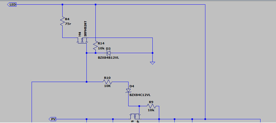
The gate of Q7 will also need some protection with a Zener diode, as the max. voltage will be exceeded if DCDC_LOAD(LED)_OUT is pulled down to GND.
Yes, Q2 can be used for booth buck or boost but once the converter is idle (for example on sunset or sunrise when there is not enough solar energy to charge a battery but a LED light not needed) Q2 will switch off hence Solar- to GND is disconnected and floating so it is not possible to measure the solar voltage anymore. I need to monitor the solar panel continuously to be able to decide when to switch on or off the LED.
Thanks for the info about the earlier protection circuit. I was trying to simulate it earlier and was not working as expected but I thought I might be wrong because it is a proven circuit
It looks like I need to find another solution to monitor the PV even in idle mode and also a protection circuit.
I’m wondering if you also tried your smaller MPPT 1210 in boost mode? Does the fw support it?
On another thread I read that you may have some blank PCBs for the MPPT 1210 (also 2420-LC maybe?). I might be interested in both if you still any, it would be easier to start development on real hw.
Imagine you are in boost mode and the voltage DCDC_IN is at 40V vs. GND. Now if ~LED_EN = 1, Pin 3 of T2 and the anode of D6 are at GND potential. The Zener diode D6 drops the reverse bias voltage of approx. 10V, so the cathode of D6 = gate of Q5 will be at -30V vs. its source, which is more than the absolute maximum of ±20V.
I just picked up the shipment this week. Many thanks for the PCB’s!
Back to your earlier observations, I think you missed that LED_EN logic is inverted.
When boost mode is used to drive an LED, T2 should be kept OFF, so LED_EN will be at 0V, in this way gate of Q6 will be pulled high through R20 an it will switch ON, finally the LED(-) will get it’s GND.
D6 anode will not be at potential 0, it will be in series with D7 so the total bias voltage will be approx 2x10V=20V so the cathode of D6, gate of Q5 will be at 20-40=-20V vs. its source. The circuit should work fine up to 40V.
We could use BZX84C12 for example and the circuit should operate safe in 34-44V range in boost mode.
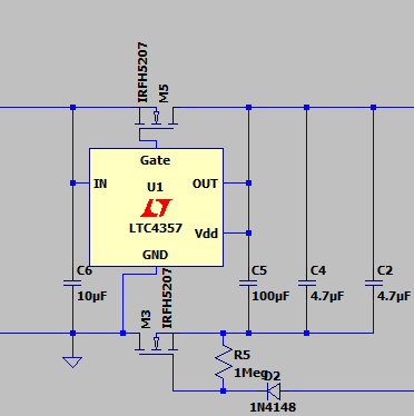
Another option could be to add a diode controller like LTC4357 for Q5, this will help to get rid of the above described limitations.
You are right, in boost mode it should be fine. However, in buck mode (LED_EN at 3.3V) you would still have a too high voltage difference at Q5 gate as soon as the solar voltage is above around 30V. Not much difference in case of 12V Zener. Maybe this issue could be solved with a resistor placed in series with the Zener diode… but didn’t check in detail.
Yes, ideal diode controller is also an option. But not the cheapest, I guess.
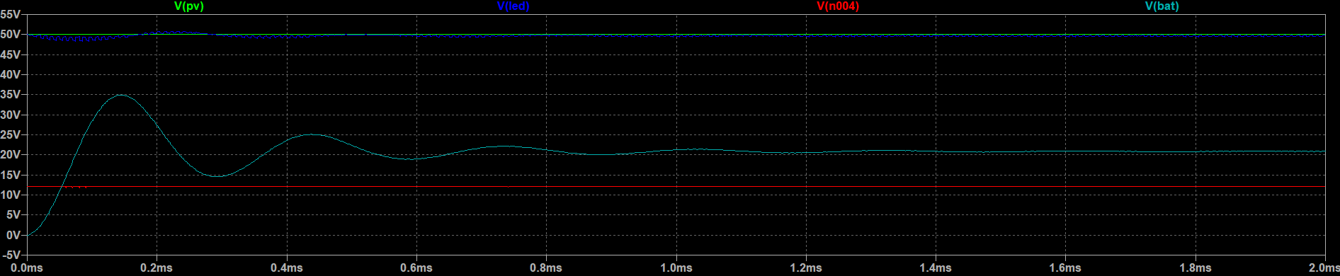
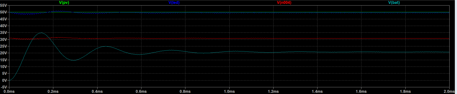
Now that we sorted out some hw issues I will build a test config to give a try.
Meanwhile I also need to study the firmware more deeply.
I found that dcdc mode is defined in config.h “#define DCDC_MODE_INIT MODE_MPPT_BUCK”
I will need to be able to modify dc/dc mode during runtime (switch it to boost on evening, and back to buck in the morning) so I’m wondering if there is a safe way doing this?
The nanogrid mode also switches dynamically between boost and buck depending on the voltage at high voltage side, so that should be possible.
The difference between boost and buck mode is mainly that the control target changes. The DC/DC always tries to control the output port current/voltage setpoints while taking care that the limits at the input are not exceeded. So if you change dcdc.mode dynamically during operation it would change its control target. (in buck mode, output control target is LV side)
The safest way would be to switch off the DC/DC first (dcdc.enable = false), then change the settings of HV and LV ports and then switch on the DC/DC in the correct mode again.
I know it’s a little bit off-topic but I have trouble uploading the fw with my original ST-link V2.
Configuring upload protocol…
AVAILABLE: blackmagic, jlink, mbed, stlink
CURRENT: upload_protocol = stlink
Uploading .pio\build\mppt-1210-hus-v0.7\firmware.elf
xPack OpenOCD, 64-bit Open On-Chip Debugger 0.10.0+dev (2019-07-17-11:28)
Licensed under GNU GPL v2
For bug reports, read http://openocd.org/doc/doxygen/bugs.html
Info : The selected transport took over low-level target control. The results might differ compared to plain JTAG/SWD
srst_only separate srst_nogate srst_open_drain connect_deassert_srst
Info : clock speed 300 kHz
Info : STLINK V2J29S7 (API v2) VID:PID 0483:3748
Info : Target voltage: 1.087328
Error: target voltage may be too low for reliable debugging
Info : stm32l0.cpu: hardware has 4 breakpoints, 2 watchpoints
Info : Listening on port 3333 for gdb connections
Info : Unable to match requested speed 300 kHz, using 240 kHz
Info : Unable to match requested speed 300 kHz, using 240 kHz
target halted due to debug-request, current mode: Thread
xPSR: 0xf1000000 pc: 0x08001a50 msp: 0x20005000
STM32L0: Enabling HSI16
Info : Unable to match requested speed 2500 kHz, using 1800 kHz
Info : Unable to match requested speed 2500 kHz, using 1800 kHz
** Programming Started **
Info : Device: STM32L0xx (Cat.5)
Info : STM32L flash has dual banks. Bank (0) size is 96kb, base address is 0x8000000
Error: jtag status contains invalid mode value - communication failure
Info : Previous state query failed, trying to reconnect
Error: error writing to flash at address 0x08000000 at offset 0x00000000
embedded:startup.tcl:449: Error: ** Programming Failed **
in procedure ‘program’
in procedure ‘program_error’ called at file “embedded:startup.tcl”, line 508
at file “embedded:startup.tcl”, line 449
*** [upload] Error 1
I spent some time to find out why my original programmer is not working but couldn’t actually find an explanation.
For anyone facing similar problem, the only way to get it working in may case is to simply let an original tool like STM32 ST-LINK utility or STM32CubeProgrammer running in the background. No need to connect to the programmer, just simply let it running. It may be a usb power management issue or whatsoever…I may spend some more time on debugging later.
Meanwhile I also started to study the fw more deeply but is quite sophisticated so I definitely will need quite some time to understand it in all it’s aspects. @martinjaeger, do you have some more detailed docs, flowcharts etc?
If there is someone who already knows more about the fw and willing to contribute and help me to implement my idea is welcome to this thread.
I already have working prototypes but uses different hw and architecture and I can share the logic behind it and many more details to get it running on this hw.
@martinjaeger
I was just thinking that this LED driving feature could also be implemented in your new 20A MPPT. No plans to implement such a feature in your new design?